TL;DR: Chinese Engineering has surpassed Western Engineering
Introduction
I’ve shown some interest in Car Chargers in the past:
Tuning a dual usb car charger
Quick Charge
But the time goes on and today we apparently need Quick Charge to surpass the measly 5V 500mA of the original USB Standard.
Quick Charge 3.0
Quick Charge is a relatively simple protocol which you can implement by Bit-Banking the D+ and D- USB lines. With this protocol, you can set the output voltage from 3.6 V to 20 V in 200mV increments. Maximum current is 4.6A and 3A @12V. This gives us 36W over an unmodified USB Cable with no danger of destroying legacy or non-QC devices.
Quick Charge 4.0
Things get murky here. What I’ve found:
- Decreased step width from 200mV to 20mV
- Voltage range stays the same from 3.6V to 20V
- unsure: 0A to 3A in 50mV steps
Essentially this is a programmable power supply.
Implementing Quick Charge
This is much easier than USB-PD. You just manipulate the D+ and D- lines. All that’s needed is an Arduino: http://blog.deconinck.info/post/2017/08/09/Turning-a-Quick-Charge-3.0-charger-into-a-variable-voltage-power-supply
With USB-PD there is some serios stuff going on
- Powerline Communication over the VCC lines
- Verification of the insertion angle of the USB cable
- Communication over the CC wires
FIVI Car Charger
Well, that’s what the device calls itself. It’s $4.15 incl. shipping at Aliexpress: https://www.aliexpress.com/item/32988560675.html
I suspect that this device is available from all kinds of resellers with different names.
Specifications:
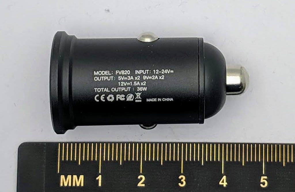
- All metal case
- Tiny! This gets lost in the car socket
- Dual output with 36W total
- QC 3.0
- Maximum 24V input (untested)
Outer appearance
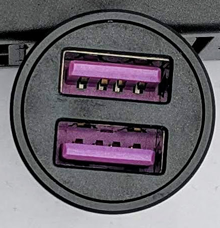
View from top. Both outputs are QC 3.0 capable.
Disassembly
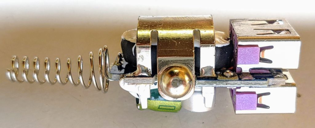
The casing was difficult to open. You have to turn the whole PCB assembly inside the device by applying torque at the USB slots. The Ground pins will get pulled inside the casing. Afterwards, you can pull the PCB out at the USB slots. There is a black cover over the USB Ports which is held in place by clamps. Just pull it out with brute force.
PCB
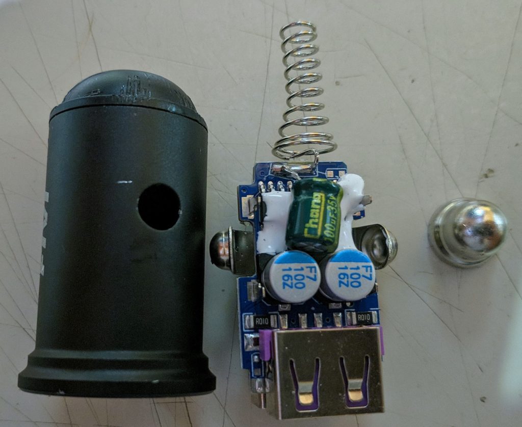
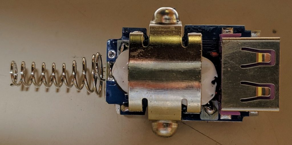
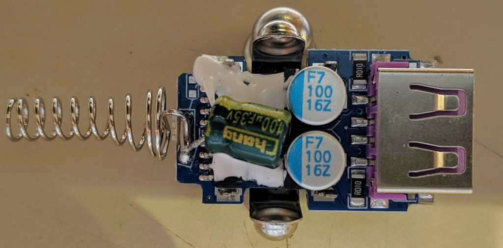
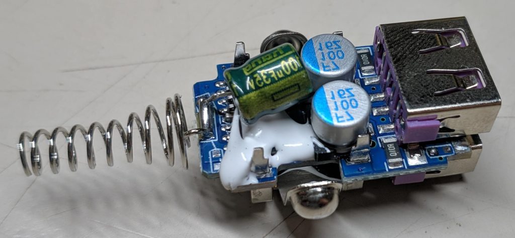
Unfortunately, everything is covered in gunk. All I can seee are
- Input and Output Capacitors
- 2 10mΩ reistors. Which means that this is either a Cycle-by-Cycle Buck Converter or it’s a simple current measurement
- 2 relatively big inductors. Big as in “big for Chinese” because usually inductors are realized by a wiggled PCB trace
The unit is really compact and stable. Not much space is left. From my point of view this is good engineering.
Measurements
Let’s do some Measurements!
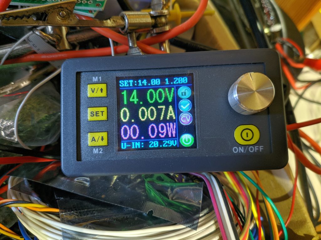
I’ve bought another DPS3005. Those are useful little buck converters with a small display which shows voltage and current consumption. Internally that thing just delivers target values to a TL494.
Idle is just 100mW. Not too shabby! That makes it useful for some battery applications. The Power Supply is very inexact at these levels.
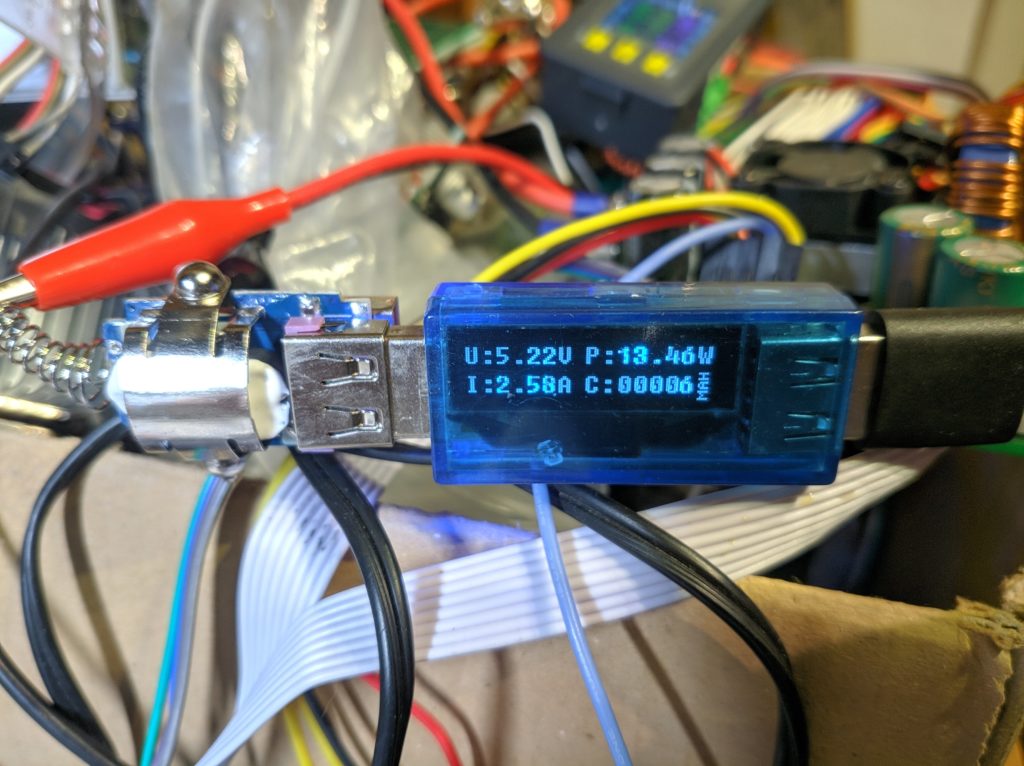
If you disable the Quick Charge part you’re left with 5V. With crappy cables this delivers 2.38A to my smartphone. If we do the math for Input / Output wattage we even have an overunity device! Or maybe it’s just inaccuracies.
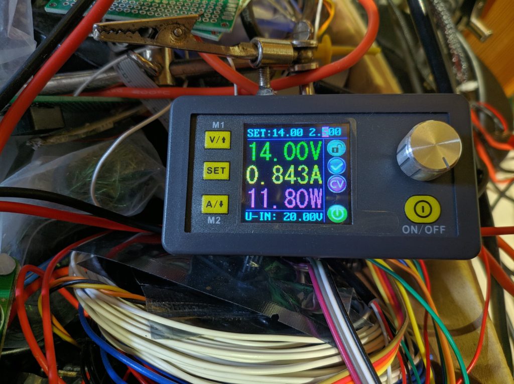
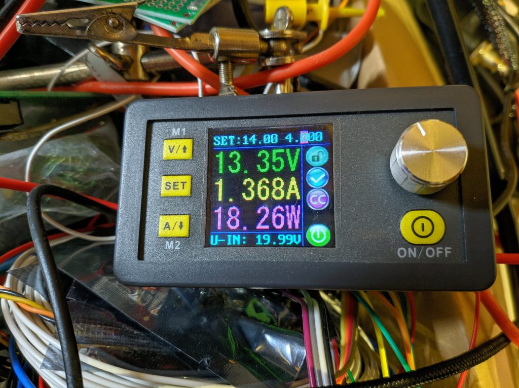
Here it is Quick Charging my Xiami Mi Mix 2 with a rundown battery. Unfortunately the DPS3005’s regulation is also pretty crappy, so we have some osciallations here which make measurements difficult.
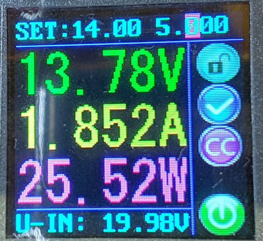
And here the less than thumb-size charger is pumping in 25W into my TS80 soldering iron! That’s more than with the Aliexpress QC3.0 PCB modules. The soldering iron heats up considerably faster.
The circuit heats up to body temperature at this power level. So it’s also very efficient.
Conclusion
Crazy. In just a few years Chinese engineering advanced from a simple resistor and relying on the phone’s protection circuit to this little marvel which gets shipped next to nothing around the globe. If I was to develop such an device I’m not sure that I could meet this goal.
